Question about Voltage Doubler
페이지 정보
작성자 김준하 댓글 2건 조회 682회 작성일 20-04-21 15:03본문
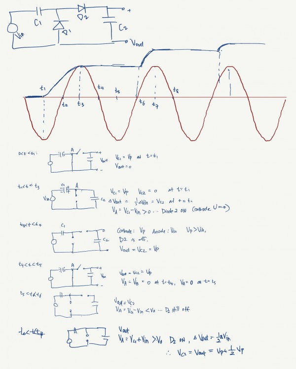
From the attached figure, from t6 to t7, D2 turns on because its anode (V_C1 + V_in) is larger than the cathode (V_C2 = V_p).
This makes Capacitor 2 gain half of the input voltage change (by voltage division), thus resulting in V_out = V_p + 1/2(V_p).
The thing that I am curious about is whether this increase in voltage across C2 is due to the input voltage or due to C1 discharging.
If C1 is discharging, does that mean the voltage across C1 drops to 1/2(Vp)? Or do we have to assume that the time constant for both capacitors are so large that no discharging occurs during this process?
댓글목록
TA님의 댓글
TA 작성일
It seems the timing diagram you drew is quite incorrect.
In the first negative cycle, D1 is on so C1 is charged up to Vp.
Then in the following positive cycle, D1 is off and D2 is on.
So, C1 discharges and C2 charges, which is an answer to your first question.
Voltage across C2 increases until D2 is finally off and no charging path is given.
Therefore, final voltage is 2Vp, not Vp + 1/2Vp. (Vp by voltage source, another Vp by C1)
김준하님의 댓글
김준하 작성일
Thank you for your response! I have put the analysis above referring to the textbook.
According to the textbook, the voltage doubler's output voltage is stated to increase in a geometric series with a common ratio of 1/2.
So using the infinite sum of the sequence, V_p/ (1-1/2), we get 2V_p.
Can we ignore this geometric series and assume the process that you have provided us explains the process accurately?
