
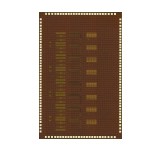
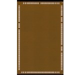
2014
EEG-Connectome Chip
Technology
Chip Size
Power Supply
Function
Channel Frequency
Power Consumption
Released Date
0.18 μm CMOS Process
1.0 mm x 3.8 mm
1.8V
EEG-Connectome Processing
20MHz
1.71mW
Dec. 2014
|
2014
EEG-Connectome Chip
|
Technology
Chip Size
Power Supply
Function
Channel Frequency
Power Consumption
Released Date |
0.18 μm CMOS Process
1.0 mm x 3.8 mm
1.8V
EEG-Connectome Processing
20MHz
1.71mW
Dec. 2014 |
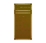
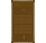
2014
BONE-AR
Technology
Chip Size
Power Supply
Function
Injection Method
Injectable Current
Frame Rate
Power Consumption
Released Date
0.18 μm 1P6M CMOS Technology
2.5 mm x 3.8 mm (including pads)
1.5 V
Electrical Impedance Tomography (EIT)
Dual Frequency Division Multiplexing
125-500μAp-p (10~360kHz)
30fps
4.84mW
Dec. 2014
|
2014
BONE-AR
|
Technology
Chip Size
Power Supply
Function
Injection Method
Injectable Current
Frame Rate
Power Consumption
Released Date |
0.18 μm 1P6M CMOS Technology
2.5 mm x 3.8 mm (including pads)
1.5 V
Electrical Impedance Tomography (EIT)
Dual Frequency Division Multiplexing
125-500μAp-p (10~360kHz)
30fps
4.84mW
Dec. 2014 |
2014
M3H
Technology
Chip Size
Power Supply
Function
Key Accelerators
Power Consumption
Released Date
0.11 μm Dongbu CMOS Process
3.375 mm x 2.25 mm
1.2V, 3.3V
Multimodal Mental Management System IC
Electroencephalography sensor, Near-infrared Spectroscopy sensor
24mW @ maximum condition
Aug. 2014
|
2014
M3H
|
Technology
Chip Size
Power Supply
Function
Key Accelerators
Power Consumption
Released Date |
0.11 μm Dongbu CMOS Process
3.375 mm x 2.25 mm
1.2V, 3.3V
Multimodal Mental Management System IC
Electroencephalography sensor, Near-infrared Spectroscopy sensor
24mW @ maximum condition
Aug. 2014 |
2014
DMLP
Technology
Chip Size
Power Supply
Function
Key Block
Power Consumption
Released Date
65 nm 1P8M CMOS Process
2.5 mm x 4.0 mm
1.2V
Deep Learning and Inference
DLE, DIE, TRNG
185.3mW
Aug. 2014
|
2014
DMLP
|
Technology
Chip Size
Power Supply
Function
Key Block
Power Consumption
Released Date |
65 nm 1P8M CMOS Process
2.5 mm x 4.0 mm
1.2V
Deep Learning and Inference
DLE, DIE, TRNG
185.3mW
Aug. 2014 |
2014
Biocle A
Technology
Chip Size
Power Supply
Function
Modulation
Channel Frequency
Sensitivity
Power Consumption
Released Date
65nm CMOS Technology
1.8 mm x 3.2 mm
1.2V
Body Channel Communication Transceiver
BPSK, OOK
40MHz(40MHz BW), 160MHz(40MHz BW), 13.56MHz(100kHz BW)
-58dBm @ 80Mb/s, -72dBm @ 100kb/s
79pJ/b, 42.5μW
Aug. 2014
|
2014
Biocle A
|
Technology
Chip Size
Power Supply
Function
Modulation
Channel Frequency
Sensitivity
Power Consumption
Released Date |
65nm CMOS Technology
1.8 mm x 3.2 mm
1.2V
Body Channel Communication Transceiver
BPSK, OOK
40MHz(40MHz BW), 160MHz(40MHz BW), 13.56MHz(100kHz BW)
-58dBm @ 80Mb/s, -72dBm @ 100kb/s
79pJ/b, 42.5μW
Aug. 2014 |

2014
NT-FMP
Technology
Chip Size
Function Supply Voltage
Power Consumption
Operating Frequency Released Date
65 nm CMOS Process
4 mm x 0.5 mm
Ultra-low-power Object Matching Processor
0.5V(Logic), 0.8V(SRAM)
54μW
5MHz
|
2014
NT-FMP
|
Technology
Chip Size
Function Supply Voltage
Power Consumption
Operating Frequency Released Date |
65 nm CMOS Process
4 mm x 0.5 mm
Ultra-low-power Object Matching Processor
0.5V(Logic), 0.8V(SRAM)
54μW
5MHz
|
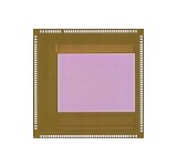
2014
Gaze Image Sensor (GIS)
Technology
Chip Size
Power Supply
Function
Frequency
Peak Performance
Power Consumption
Released Date
65 nm 1P8M CMOS Process
3.36 mm x 3.36 mm
2.5V (Pixel), 1.2V (Other)
Gaze Image Sensor
50MHz
0.3 GOPS
10mW(Average), 34mW(Peak)
Jun. 2014
|
2014
Gaze Image Sensor (GIS)
|
Technology
Chip Size
Power Supply
Function
Frequency
Peak Performance
Power Consumption
Released Date |
65 nm 1P8M CMOS Process
3.36 mm x 3.36 mm
2.5V (Pixel), 1.2V (Other)
Gaze Image Sensor
50MHz
0.3 GOPS
10mW(Average), 34mW(Peak)
Jun. 2014 |

2014
Object Recognition Processor (ORP)
Technology
Chip Size
Power Supply
Function
Frequency
Peak Performance
Power Consumption
Released Date
65 nm 1P8M CMOS Process
4.0 mm x 4.0 mm
1.2V (Normal), 0.7V~1.2V(DVFS)
Object Recognition
50MHz(DGP), 100MHz(FDP/SSP/FMP),
200MHz(CNNP/DRMP/EOGP/FA/NoC)
151 GOPS
65mW(Average), 97mW(Peak)
Jun. 2014
|
2014
Object Recognition Processor (ORP)
|
Technology
Chip Size
Power Supply
Function
Frequency
Peak Performance
Power Consumption
Released Date |
65 nm 1P8M CMOS Process
4.0 mm x 4.0 mm
1.2V (Normal), 0.7V~1.2V(DVFS)
Object Recognition
50MHz(DGP), 100MHz(FDP/SSP/FMP),
200MHz(CNNP/DRMP/EOGP/FA/NoC)
151 GOPS
65mW(Average), 97mW(Peak)
Jun. 2014 |